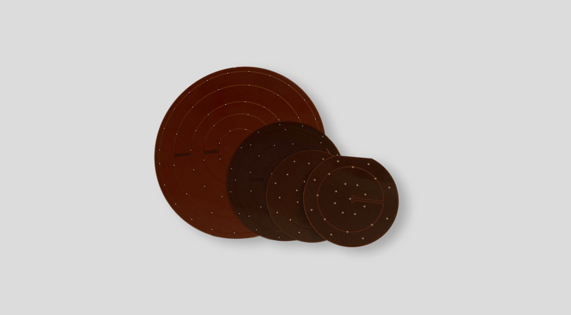
During wafer test processes strong bowed wafers are at a major risk of breakage. In addition, a good contact to the base chuck is needed during wafer testing operation. The new Wafer Test T-ESC® is a perfect solution to handle this problem. The thin and bowed wafer is fixed by the Electrostatic Wafer Test T-ESC® and kept flat. Now the package can be loaded into the wafer test tool. In the wafer test process the second advantage comes into play, the front and back side of the Carrier are electrically connected.
Therefore, a highly conductive path from the tool chuck to the wafer back side is given. This means that the operation of the wafer test tool is not affected by the usage of the Wafer Test T-ESC®. The measurement can now also be used for thinned and warped wafers in a perfect way. The mobile bipolar Wafer Test T-ESC® is available for all wafer sizes and shapes and it can also be used for wafer piece. Get your quote now!