


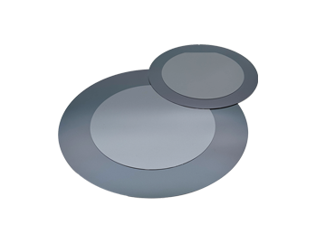
Transferable Electrostatic Carriers
The Transferable Electrostatic Carrier (T-ESC®) is an adhesive-free temporary bonding method that enables the safe and reliable processing of fragile substrates and various materials such as ultra-thin substrates, GaAs, InP, LN, LT, thin silicon, thin MEMS wafers and many more. The basic concept behind this sustainable temporary bonding technology involves the use of electrostatic forces to chuck device wafers onto mobile rigid Carriers (T-ESC®).
These wafer-carrier packages can then be handled and securely processed like wafers of standard thickness through existing machines within the customer facility. Therefore, existing cassettes, handling tools and fabrication equipment can be used without modifications. Additionally, the warping and bowing of thin and ultra-thin substrates are eliminated. The Transferable Electrostatic Carriers are available in the standard sizes from 2" to 12" and in customized shapes adapted to the intended application.
The Adapter Carrier
Each T-ESC® type is offered as an adapter version that allow machines to process device wafers of different diameters and forms. The smaller device wafer can be temporarily bonded to an Adapter Carrier and is held in position by electrostatic forces. For example, a 4”/8” Adapter T-ESC is suited to fixate a 4” wafer on an 8” Adapter T-ESC.
The package of a 4” wafer and an 8” Adapter Carrier can now be used in the intended equipment, e.g. an 8” Stepper. The Stepper tool recognizes a standard 8” substrate and can now process the smaller 4” wafer sizes.
(MEMBER OF THE T-ESC® FAMILY)
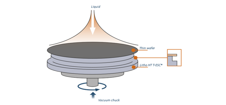
Litho HT T-ESC®
The Lithography High-Temperature Transfer ElectroStatic Carrier (Litho HT T-ESC®) is our specifically designed solution for thin wafer handling support during whole lithography processes containing the different steps. It is based on our HT T-ESC®, due to a special design liquid between T-ESC® and wafer is avoided which enables lithography processing with high yields.
There is also an adapted version available for the so called slide off debonding process mainly used for compound semiconductors such as GaAs, InP, etc.
Typical Applications
-
Solution for thin wafer handling support during lithography processes
-
High temperature (up to 400°C) and vacuum-suited
-
Compatibility with existing handling systems (transport cassettes, vacuum, Bernoulli or mechanical end effectors, etc.)
-
Ultra low contamination
-
High flatness
-
Outgassing free
-
Reusable
-
Sizes from 2" to 12", customized shapes and features possible
Recommended Processes
-
Spin Coating
-
Baking (Soft & Hardbake)
-
Exposure
-
Developing
-
Resist Stripping
-
Single Wafer Spin Etching
-
Slide Off De-Bonding
-
Handling
(Single Wafer) Spin Etching
Spin etching is following the same principle as spin coating. The substrate is clamped to a chuck and during the spinning, etching chemicals are jetted to the surface.
Handling
During the wafer processing the wafer needs to be transferred back and forth from the cassettes to the tools and also inside the tools from one station to the other. For fragile substrates this is already challenging, because they tend to break or get cracks, which can lead to future breakage. Also the bowing of thinned substrates brings a lot of trouble for all tooling because they are usually not designed for this very special operation. Temporary bonding with our T-ESC® is a great help here as the processing tools only see a standard wafer and trouble with handling. Therefore, wafer breakage is eliminated.
Lithography
Lithography is the general naming of the complete lithography processing steps such as coating, bake, exposure etc.
Spin Coating
Part of the Lithography processing, while the substrate is clamped on a chuck liquid chemicals are sprayed or jetted on to its surface. The substrate is rotating during this procedure or after it, so that the chemicals are spread equally across the surface.
During Spin Coating a non uniform edge builds up at the wafer edge. This edge may cause problems during further processing and therefore needs to be removed which is called Edge Bead Removal.
Baking
During Lithography processing several baking steps are required to achieve the optimal grade of the resist to withstand the following substrate etching processes and to achieve the targeted structure in the end. Baking basically means that the substrate together with the coating is heated to a specific temperature. This is kept for a while and afterwards the substrate is cooled down and ready for the next step.
Exposure
The already coated wafer is irradiated by light or other irradiation sources through a mask. Thus, structures can be formed later out of this pattern.
Resist Developing
To generate a real structure out of the exposed coating, the coating is partially removed by a developing agent. This can be done either in a bath or again by a spinning type of tool. For our mobile electrostatic carriers we recommend to only use spinning tools. After the development stage the pattern is visible at the coating and the substrate can get structured in the patterned region after the baking procedure.
Resist Stripping
Not needed or unwanted photoresist is removed in the resist stripping process. This is usually done by chemicals. The dry stripping process is also possible. Please refer to plasma clean/ashing.
Slide-Off De-Bonding
Slide-Off De-Bonding is used when a fragile wafer is glued to a temporary carrier and needs to be released with the Slide-Off De-Bonding after the processing. The glued carrier combined with the substrate is heated until the glue gets liquid. Then the wafer or the carrier slides in one direction whereas the other is fixed in position. Afterwards the glue residues on the wafer have to be removed by chemicals. The whole process can be supported by our mobile electrostatic carrier (T-ESC®) and the thin wafer always has a rigid support during Slide-Off and the later cleaning step.
Our Machines
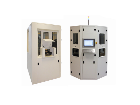
ACU 3000
A fully automated electrostatic chucking/ dechucking unit with up to 120 wafers and/or T-ESC® packages per hour, guaranteeing the highest yield during handling and many diagnostics features.
Learn More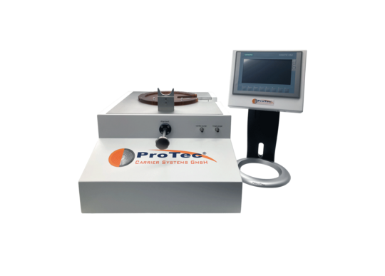
MCU 3000
A manual chucking/ dechucking unit of thin and ultra-thin substrates on carriers (T-ESC®s) for flexible sizes from 4”/6” to 8”/12” with a high flexible mobile handling tool and diagnostics features.
Learn More