Electrostatic Chuck (ESC)
The ESC technology by ProTec® offers the solution for demanding processing on new or even existing equipment, leading to a better cost of ownership and an easy integration of new processes on already existing lines, such as thin glass coating on standard equipment. Highest yield also for fragile substrates can be generated for inline- and also cluster-based processing tools.
Our electrostatic fixation systems are specifically designed to the needs of our customers, e.g. chucking multiple glasses (also 3D type) on a mobile electrostatic carrier and guiding them through an inline plasma coating step or for temperature-controlled wafer processing during demanding plasma steps.
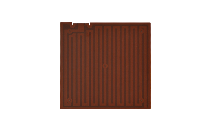
Polymer Electrostatic Chuck
ProTec®'s polymer electrostatic chucking solutions are used in low temperature vacuum and atmospheric processes for chucking wafers, glasses or foils. The design is customized to your specific needs. Even 3D shapes are possible allowing the substrate to be fixed in the desired configuration. The chucking procedure can be done either under atmosphere or inside vacuum and the transfer between both is always possible, so that e.g. an optical bonding application with thin glasses or foils can also be done in vacuum environment. Depending on the application the polymer electrostatic chuck can be used in inline or cluster-based systems.
Polymer Electrostatic Chuck
Typical Applications
-
100% customized in size, shape, functionality to best customer benefit
-
Size starting from very small 10x10mm² to large formats like Gen 10.5
Recommended Processes
-
Handling
-
Optical Bonding
-
Substrate Bending
Optical Bonding is used for different reasons in the display manufacturing process. It can help to make the fragile glass more robust while still maintaining a good picture quality or enhancing the readability outdoor. Basically, the process describes a method to bond an optical active (e.g. transparent) substrate with another one by glue. In combination with our T-ESC® technology the process can be carried out in vacuum to enhance the results.
During the wafer processing the wafer needs to be transferred back and forth from the cassettes to the tools and also inside the tools from one station to the other. For fragile substrates this is already challenging, because they tend to break or get cracks, which can lead to future breakage. Also the bowing of thinned substrates brings a lot of trouble for all tooling because they are usually not designed for this very special operation. Temporary bonding with our T-ESC® is a great help here as the processing tools only see a standard wafer and trouble with handling. Therefore, the wafer breakage is eliminated.
During various processes a substrate needs to be shaped according to the customers' needs. In some cases it needs to be flat, in others it should follow a given shape and stay fixed over the process time.
Our Machines

ACU 3000
A fully automated electrostatic chucking/de-chucking unit with up to 120 wafers and/or T-ESC® packages per hour, guaranteeing the highest yield during handling and many diagnostic features.
Learn More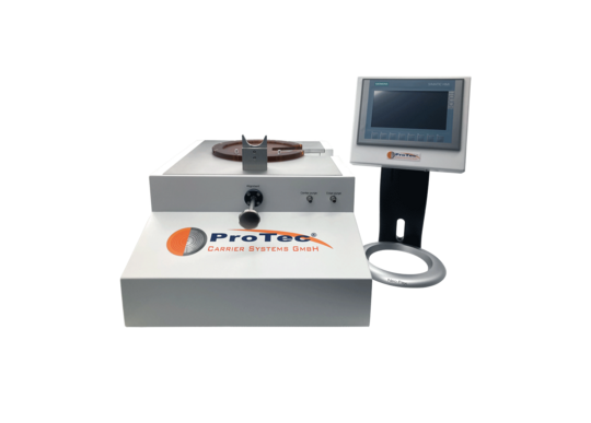
MCU 3000
A manual chucking / de-chucking unit of thin and ultra-thin substrates on carriers (T-ESC®s) for flexible sizes from 4”/6” to 8”/12” with a high flexible mobile handling tool and diagnostic features.
Learn More