Semiconductor
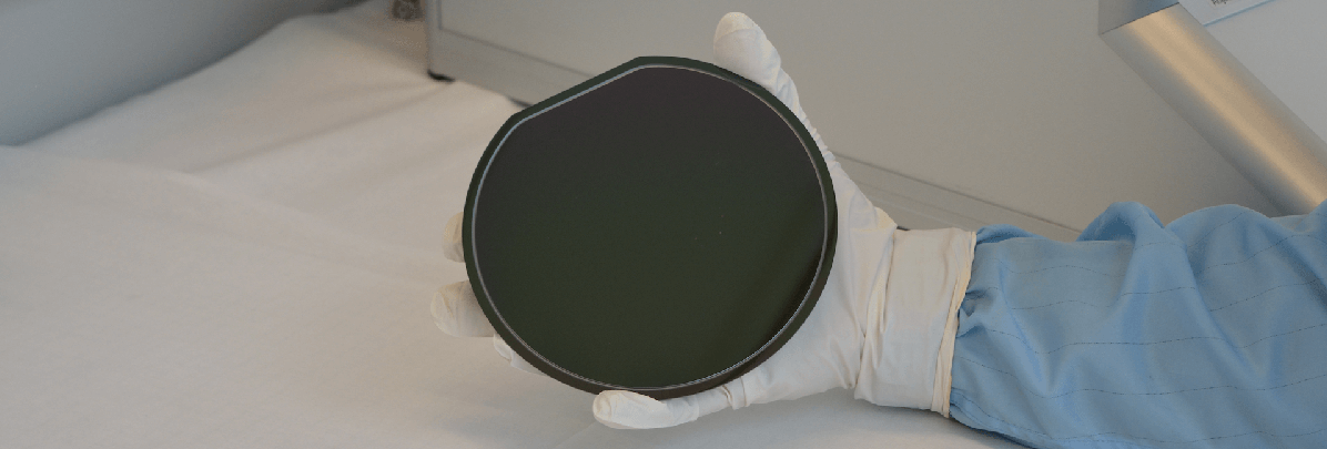
The T-ESC® Technology by ProTec® offers safe and easy handling as well as processing of fragile, thin and ultra-thin substrates (thinner 50 µm), e.g. GaAs, InP, LN, LT, thin silicon, thin MEMS wafer and many more. The basic concept behind this adhesive-free temporary bonding technology involves using electrostatic force to chuck thin and ultra-thin wafers onto mobile rigid Carriers (T-ESC®). Such wafer-carrier packages can be handled and processed like wafers of standard thickness.
Therefore, existing standard cassettes, handling tools and fabrication equipment can be used without modifications. Additional effect: The warping and bowing of thin and ultra-thin substrates are eliminated, which is highly welcome. All of our Carriers are available in standard sizes from 2" to 12" and additionally in customized shapes suited to the intended application.
(MEMBER OF THE T-ESC® FAMILY)
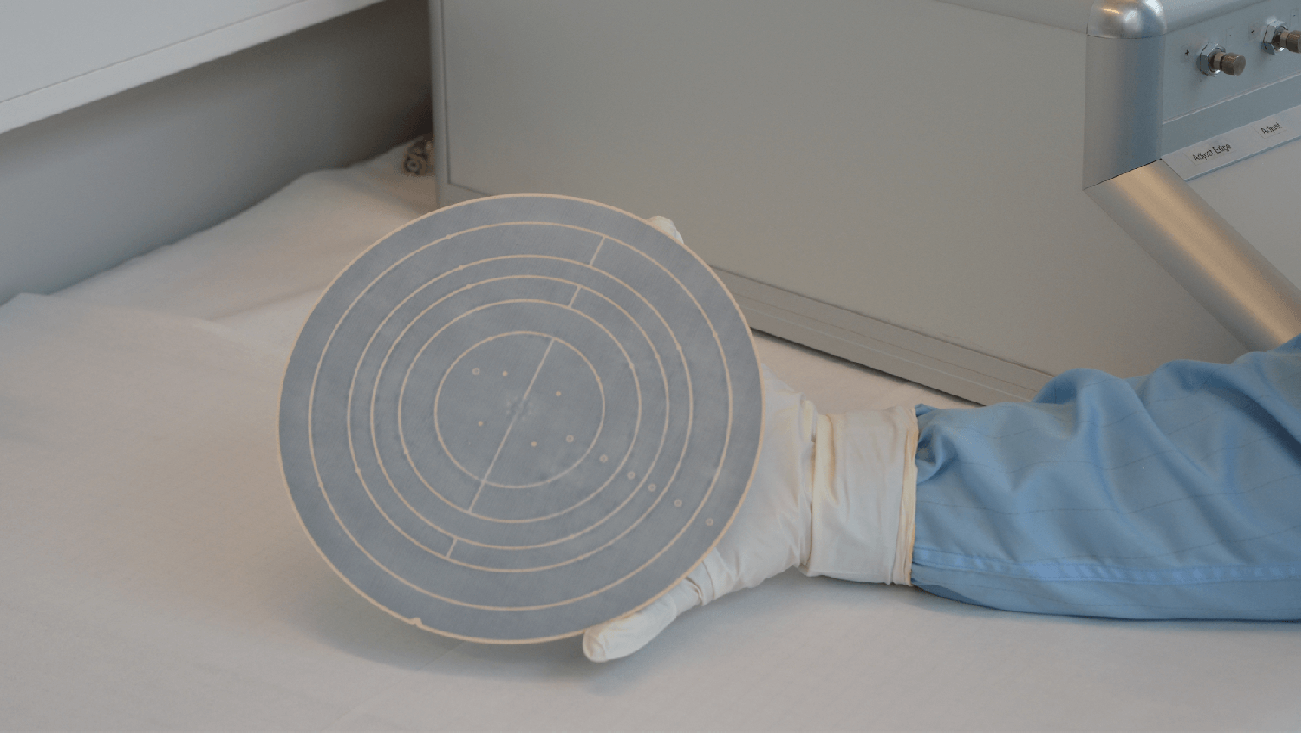
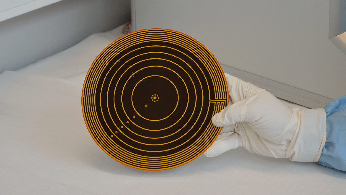
Glassfiber T-ESC®
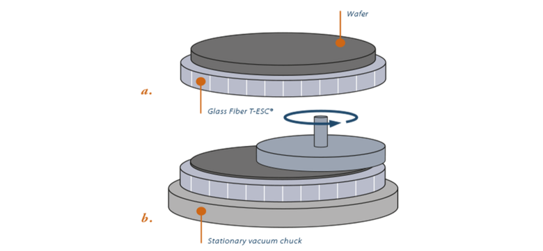
The Glassfiber Transfer ElectroStatic Carrier (Glassfiber T-ESC®) enables temporary bonded wafer thinning without the need of adhesive, starting from a thick wafer grinding down to ultra thin wafer thickness. This mobile rigid wafer support helps to generate high yield even when going to the ultra thin wafer thicknesses. Furthermore this mobile electrostatic Carrier can be used in process applications such as handling and probing.
Glassfiber T-ESC®
Typical Applications
-
Compatibility with existing handling systems (transport cassettes, vacuum, Bernoulli or mechanical end effectors, etc.)
-
High flatness
-
Re-usable
-
Sizes from 2" to 12", customized shapes and features possible
Recommended Processes:
-
Grinding
-
Handling
-
Probing
Grinding
Grinding is a substrate thinning process, where material is mechanically removed.
During wafer processing the wafer needs to be transferred back and forth from the cassettes to the tools and also inside the tools from one station to the other. For fragile substrates this is already challenging, because they tend to break or get cracks, which can lead to future breakage. Also bowing of thinned substrates brings a lot of trouble for all tooling because they are usually not designed for this very special operation. Temporary bonding with our T-ESC® is a great help here as the processing tools only see a standard wafer and trouble with handling. Therefore, the wafer breakage is eliminated.
Various probing methods exist. They are used to check the substrate´s or device´s functionality, e.g. there are optical inspection or electrical probing.
Our Machines
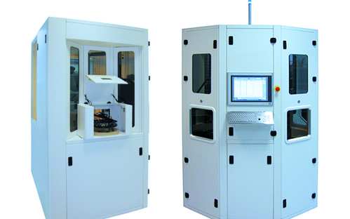
ACU 3000
A fully automated electrostatic chucking/de-chucking unit with up to 120 wafers and/or T-ESC® packages per hour, guaranteeing the highest yield during handling and many diagnostics features.
Learn More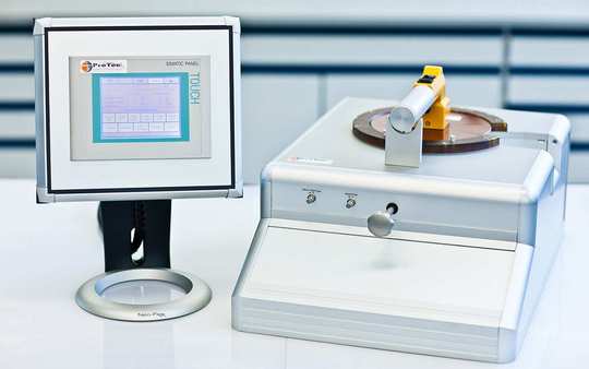
MCU 3000
A manual chucking / de-chucking unit of thin and ultra-thin substrates on carriers T-ESC® for flexible sizes from 4”/6” to 8”/12” with a high flexible mobile handling tool and diagnostics features.
Learn More